1. Which of the following configuration is used as input stage of the multistage amplifier?
a) Common base configuration
b) Common emitter configuration
c) Common collector configuration
d) All configurations are equally suited
Explanation: Since input resistance is low and output resistance is high common base configuration is used as an input stage of the multistage amplifier. Common emitter configuration is used for audio signal amplification. Common collector is used for impedance matching.
2. Which of the following configuration is used for audio signal amplification?
a) Common base configuration
b) Common emitter configuration
c) Common collector configuration
d) All configurations are equally suited
Explanation: Common base configuration is used as input stage of multistage amplifier since it has low input resistance and high output resistance. Since voltage gain is high, common emitter configuration is used for audio signal amplification. Common collector is used for impedance matching since the voltage gain is unity.
3. Which of the following configuration is used for impedance matching?
a) Common base configuration
b) Common emitter configuration
c) Common collector configuration
d) All configurations are equally suited
Explanation: Common base configuration is used as input stage of multistage amplifier since it has low input resistance and high output resistance. Since voltage gain is high, common emitter configuration is used for audio signal amplification. Common collector is used for impedance matching since the voltage gain is unity.
4. At saturation, which of these is not true for a BJT?
a) The collector current IC cannot increase further
b) The base current IB, cannot increase further
c) The collector-to-emitter voltage, VCE is due to the non-zero internal resistance of BJT
d) VCE(saturation) is the minimum voltage drop between C and E
Explanation: At saturation, the collector-to-emitter voltage is the minimum drop possible occurring due to the non-zero internal resistance of the BJT. Since it cannot decrease further, the current IC cannot increase further. The BJT is said to be saturated. However, the base current, IB, can keep increasing with the input voltage and hence, in saturation, the relation IC = βIB is not satisfied.
5. For a transistor in saturation, which is true?
a) IC = βIB
b) IC > βIB
c) IC < βIB
d) IC = (β+1)IB
Explanation: At saturation, collector current remains constant. However, the base current increases with the input voltage being applied and hence BJT cannot satisfy the relation IC = βIB. In the saturation region, βIB > IC is the correct relation.
6. Given that the BJT is completely saturated, what is the overdrive?
a) Overdrive = 1
b) Overdrive < 1
c) Overdrive > 1
d) Overdrive > 0
Explanation: Overdrive during BJT saturation is the ratio of its normal β and its forced β. Forced β is the ratio of IC(sat) and IB when BJT is in saturation. Since in saturation IC is constant and IB increases thus, IC/IB decreases and the forced β is less than the normal β. Hence the overdrive > 1. In hard/strong saturation, β>>1.
7. What is the ON resistance of a transistor?
a) RON = VCEsat/βIB
b) RON = VCEsat + VA/ICsat
c) RON = VCEsat/(β+1)IB
d) RON = VCEsat/ICsat
Explanation: In the saturation region, we consider that the transistor acts as an ON switch. In this region, both collector-to-emitter voltage as well current are constant and do not change. The ON resistance is the ratio of this saturation voltage to saturation current.
8. For the graph which depicts collector current, find the ON time.
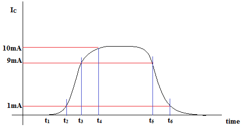
t1 = 1ms
t2 = 2ms
t3 = 4ms
t4 = 6ms
t5 = 16ms
t6 = 18ms
a) 3ms
b) 1ms
c) 2ms
d) 5ms
Explanation: On time is the time taken by BJT to change from the OFF state to the ON state. It is the sum of the delay time and the rise time. Rise time is the time taken by current to increase from 10% to 90% of saturation and delay time is time taken by current to increase from 0 to 10% of the saturation.
ton = td + tr = t2 – t1 + t3 – t2 = 2 – 1 + 4 – 2 = 3ms.
9. Which of these relations is true always for the BJT as a switch?
a) Off time >> On time
b) Off time = Storage time – Rise time
c) Off time << On time
d) Off time = Storage time + Delay time
Explanation: Off time for a BJT is larger than its ON time. Off time=Storage time + Fall time.
Often Storage time is larger than fall/delay/rise time and hence OFF time is quite large than ON time.
10. How is BJT used as a faster switch?
a) By operating it in the saturation and cut-off region
b) By operating it in the active and cut-off region
c) By using it in strong saturation
d) By decreasing its ON resistance
Explanation: If BJT is to act as a switch with negligible power dissipation, then BJT is operated in the cut-off and saturation region, as in the TTL family. When BJT has to be operated as a fast switch, then it is operated in the active and cut-off region, as in the ECL family.