1. For the given circuit, what is the minimum peak value of the output waveform if the input waveform is 10V square wave with switching time of 1 second?
Assume that the input switches between +10V and -10V DC levels.
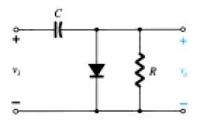
a) 0 V
b) -5 V
c) -20 V
d) -10 V
Explanation: For the positive half of the input, the diode is in the on state and hence acts as a short circuit and hence vo = 0 V. For the negative half cycle, the resistor receives voltage input both from the source and the capacitor which is charged during the positive half of the input. Hence, vo = -20 V.
2. For the given circuit and input waveform, the peak value of the output is +30V.
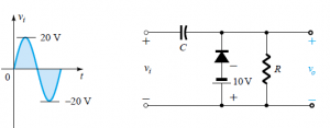
a) True
b) False
Explanation: The given circuit is a clamper with an independent DC supply of +10 V. Keeping in mind the connection of the diode and the DC supply, we see that the output waveform is clamped at +10V i.e. it shifts up by +10V. Hence, the maximum value of vo=+30 V.
3. What is the logic gate implemented in the following circuit?
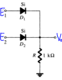
a) OR
b) AND
c) NOT
d) NOR
Explanation: In the given circuit, as a logic gate, E1 and E2 are digital inputs, 1 or 0. If the input is 1, the diode is forward biased and conducts, else it is reverse biased. So, the output is high whenever either of the input is high, or both of them are high, hence it acts as an OR gate.
4. What is the logic gate implemented in the following circuit?
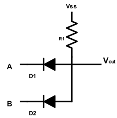
a) OR
b) AND
c) NOT
d) NOR
Explanation: Whenever either diode is forward biased, there is a path for the current to flow out of and hence the output is zero. Thus if either A or B are 0, then output is zero. If however, both A and B are equal to VSS or more, then the diodes are reverse biased and output is available. Hence the circuit acts as an AND gate.
5. Which of the following statements best describes the reason for not using diodes to implement logic gates?
a) Diodes are expensive
b) Diodes are unreliable and less efficient
c) The diode circuits have limited range of operation
d) Diodes are bulky for a logic gate
Explanation: The diode circuits are relatively less stable when compared to the transistor circuits, which are easy to tune in terms of stability and reliability.
6. In the given circuit, what is the output V0 if E1 = 10V and E2 = 0V?

a) 0 V
b) 0.7 V
c) 10 V
d) 9.3 V
Explanation: Here, current through the grounded branch = (10-0.7)/1k = 9.3 mA. Hence, voltage drop across the resistor=9.3 V. Hence, V0 = 9.3V.
7. In the given circuit, what is the ideal output V0 if E1 = 10V and E2 = 0V?
a) 0 V
b) 0.7 V
c) 10 V
d) 9.3 V
Explanation: In an ideal diode, the voltage drop is zero. Hence, complete voltage 10V appears across the resistor and as the output too.
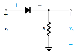
8. A 12 V, 50 Hz sine wave is fed to the given circuit as input? What is the output for 0.01s < t < 0.02s?
a) True
b) False
Explanation: The given circuit is that of a half wave rectifier in which the diode remains in the off state for the negative half and conducts for positive half. During the time 0.01 sec to 0.02sec, the input 12sin(2π50t) is positive, hence a certain output not equal to zero is available.
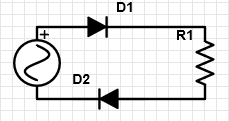
9. Which circuit has been represented in the associated circuit diagram?
a) Half wave rectifier
b) Full wave rectifier
c) NOT gate
d) AND gate
Explanation: Both the diodes are similarly biased and are in series. Hence, they form a half wave rectifier.
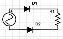
10. Which circuit has been represented in the associated circuit diagram?
a) Half wave rectifier
b) Full wave rectifier
c) NOT gate
d) AND gate
Explanation: In the given circuit, when the diode D1 is on, diode D2 is off and vice versa. Hence, the upper diode conducts during the positive half of the input cycle and the lower diode conducts during the negative half of the input cycle and hence, it is a full wave rectifier circuit.